[NDT] Non-Destructive Testing to Maximize PCBA Quality: Next-Generation QA Strategy Realized Through X-ray CT and AI Integration
- What is PCB Assembly (PCBA)?
- Standard PCBA Inspection and Quality Control Methods
- Evolving PCBA Structures and the Need for NDT
- Understanding Head-in-Pillow (HiP)
- Essential NDT Technologies for PCBA Inspection
- Conclusion: Basics
- ProLoop: Intelligent Synergy Between AOI and X-ray CT
- Insights: Deriving Conclusions with AI Automatic Judgment
- Conclusion: Advanced
- Catalog Download and Contact
[Basics] Eliminating Blind Spots in PCBA Inspection with X-ray CT:
How to Capture BGA HiP Invisible to AOI?
What is PCB Assembly (PCBA)?
PCB Assembly (PCBA) is the process of mounting and soldering various electronic components, such as ICs, resistors, and capacitors, onto a fabricated printed circuit board (PCB). This process transforms the board into a “circuit assembly” that functions as a complete electronic device based on design specifications, serving as a physical platform and power supply network.
Standard PCBA Inspection and Quality Control Methods
PCBA quality control is implemented in various ways depending on specific requirements.
- Automated Optical Inspection (AOI): Consists of high-resolution cameras, light sources, and image processing software. Designed to capture images from multiple angles as the inspection object passes through the inspection bay, these cameras take snapshots while the lighting system illuminates specific areas. The equipment’s software then processes these images and performs analysis. This system is ideal for post-reflow inspection due to its high-resolution capabilities and is highly suitable for mass production lines.
- Solder Paste Inspection (SPI): An automated quality control process used in the solder paste printing stage on a printed circuit board (PCB). This step is performed immediately after the paste is printed on the stencil and must be carried out before the pick-and-place process (component mounting) begins. Its primary purpose is to prevent defects such as insufficient or excessive solder volume and printing misalignment at the very early stages of the production line.
Evolving PCBA Structures and the Need for NDT (Non-Destructive Testing)
Currently, PCBA are becoming smaller and more complex due to multilayering. As a result, conventional visual inspection alone is insufficient.
- Increasing Complexity to Detect Defects: When defects such as Head-in-Pillow (HiP), microcracks, internal shorts, and via plating defects (voids) occur during PCB or semiconductor assembly, they are often located deep within chips or beneath components, making them difficult to detect with AOI (Automated Optical Inspection) cameras.
- Limitations of Conventional Inspection: Since even slight defects can lead to total product failure or usability issues, NDT plays an essential role in quality assurance.
- Advantages of X-ray Inspection: X-rays penetrate the workpiece to reveal internal structures such as solder joints beneath BGA chips that are beyond the reach of AOI cameras. This boosts production line confidence
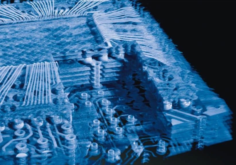
- Benefits of CT Scanning: CT Scans can be used to generate 3D images to detect internal cracks within the solder or the formation of voids in solder joints, ensuring that there will certainly be no long-term reliability issues.
Understanding Head-in-Pillow (HiP)
Head-in-Pillow (HiP) is a soldering defect where the solder ball attached to the chip and the solder paste on the PCB are in contact but fail to fuse into a single homogeneous joint.
Characteristics: This defect is invisible from the outside because the failure occurs beneath the component body. It is one of the most common defects found in modern PCB assembly.
Main Causes:
- Dynamic Warpage: As the temperature rises in the reflow oven, the BGA package or chip warps, causing the solder ball to lift away from the solder paste, preventing integration upon cooling.
- Oxidation: An oxide film on the solder ball surface or flux degradation due to improper heating prevents sufficient surface cleaning, resulting in a failure to fuse the solder.
- Improper Reflow Profile: High-temperature reflow processes can cause component twisting, leading to separation between the solder ball and paste.
Some X-ray inspection systems can be equipped with a reflow simulator on the stage inside the device, allowing for live X-ray fluoroscopic observation of the solder melting process. Please check regarding installation in Thailand.
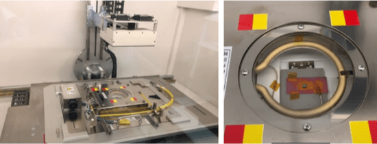
A reflow simulator attached to Comet Yxlon X-ray inspection system:
Live X-ray fluoroscopic observation of solder coalescence
Essential NDT Technologies for PCBA Inspection
How X-ray and CT scan handle these hidden joints
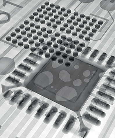
Quality inspection in the PCB post-assembly process involves examining underneath BGAs and hidden solder joints that AOI cameras cannot detect. Defects such as Head-in-Pillow (HiP) can be detected by using non-destructive testing (NDT) tools.
- X-ray Inspection: Uses oblique views (tilt angles) to check for abnormalities in solder ball shape. In a normal joint, metal density appears continuous, but in the case of HiP, slight gaps or low-density oxide layers appear as “faint separations,” or the ball is observed simply resting on the paste without collapsing.
- CT Scan: CT scan virtual slicing allows 3D models to be cut and observed at any depth (Z-axis) via software. This enables cross-sectional verification of the exact interface between the BGA ball and PCB pad. Additionally, voids and microcracks inside solder joints, which are often missed in 2D X-rays due to overlapping components, can be detected.
Conclusion: Basics
Detecting various defects in the PCB assembly process requires integrating Non-Destructive Testing (NDT) with standard inspection methods. This approach significantly reduces defect rates and enables rapid screening of anomalies. Ultimately, combining a deep understanding of the mechanisms behind defects with the selection of appropriate NDT technologies is the key to ensuring the highest level of quality and reliability for electronic products.
[Advanced] Comet Yxlon’s Smart Factory: Automating PCBA Inspection and DX with ProLoop and Insights AI
As mentioned in the first part of this article, AOI (Optical Inspection) captures surface defects at high speed but cannot see inside “hidden joints” such as those beneath a BGA. On the other hand, X-ray CT inspection reveals the “internal truth,” but CT scanning every location takes time.
Comet Yxlon resolves this dilemma by integrating ProLoop and Insights software, effectively “intelligentizing” the entire inspection process.
ProLoop: Intelligent Synergy Between AOI and the Offline X-ray CT
ProLoop serves as the command center that connects AOI and the offline X-ray CT inspection systems.
- From “Signs” to “Confirmation”: For example, when AOI detects a slight “tilt” in a BGA package, ProLoop immediately transfers those specific coordinate data to the X-ray system. The X-ray then performs pinpoint penetration to determine instantly whether it is a fatal Head-in-Pillow (HiP) defect or within an acceptable tolerance range.
- Automatic Elimination of False Failures: Only “suspected defective” gray zone areas determined by AOI are routed to precision X-ray inspection via ProLoop. This eliminates the time loss of performing 100% CT scans while removing the analog process of visual confirmation by humans, dramatically increasing the line’s First Pass Yield.
Insights: Deriving Conclusions with AI Automatic Judgment
The Insights AI analysis package renders the final judgment on the suspicious images delivered by ProLoop.
- AI Automated Decision (ADR): AI uses deep learning to automatically judge defects that are difficult for the human eye to determine, such as voids (bubbles), Head-in-Pillow (HiP), and non-wetting.
- Improved Inspection Speed: The latest version of the 3D visualization analysis software “Dragonfly” is integrated, and analysis speed is increased by up to 100 times compared to conventional methods due to GPU acceleration. Additionally, laminography (micro3Dslice) combined with AI enables high-speed automatic judgment of multilayer boards.
- 3D Metrology (Automatic Measurement): Packages like “Void Insights” allow for automatic calculation of voids in 2D/3D. Furthermore, AI identifies and measures microscopic defects at the sub-micron level (less than 1µm).
- Intuitive Operability: Compatible with the latest “Geminy UI,” providing an environment where advanced AI analysis packages (Void Insights, Review Insights) can be operated intuitively.
Conclusion: Advanced
Next-Generation Quality Assurance through Hardware and Software Fusion
By adding this intelligent software suite to Comet Yxlon’s X-ray CT inspection systems that “make the invisible visible,” PCBA factories evolve beyond mere “defect detection” to a “defect-free manufacturing process”
- Maximization of Inspection Precision: Complete quality control integrating both optical (visual) and X-ray (internal) data.
- Unmanned Operation: Elimination of human error through AI-driven automatic judgment and ProLoop’s automated system coordination.
- Minimization of Downtime: Capture predictive signs of abnormalities and feed that data back to pre-processes (such as solder printing or mounting) to break the chain of defects before they occur.
Catalog Download and Contact
Cheetah EVO is the optimal X-ray CT inspection system for PCBA manufacturing and research facilities seeking reliable high-quality inspection technology, cost-effectiveness, and maximum inspection efficiency in limited space. For more detailed information on Cheetah EVO, you can download the product catalog here.
If you are looking for effective and affordable Non-Destructive Testing (NDT) services or products for your business, please feel free to contact with us. We will be happy to provide details.
Related Information:

Non-Destructive Testing (Industrial X-ray CT Inspection) Products