
[NDT] Product Insights: FF35 CT High-Resolution Industrial CT System – Semiconductor Inspection

Equipped with the New Nanofocus Tube FYNE Tube:
A New Dimension of Non-Destructive Testing by FF35 CT
In the semiconductor and electronics industries, technological advancement knows no bounds. The miniaturization of advanced packaging technologies, represented by HBM (High Bandwidth Memory), is progressing rapidly. Consequently, the hurdles for quality assurance—specifically, how to accurately detect invisible internal defects—have risen to unprecedented heights.
The high-end X-ray CT system FF35 CT, developed by Comet Technologies (*), a global leading Swiss technology company, is a powerful solution to these industry challenges. Today, we will introduce the overwhelming benefits brought by the latest nanofocus technology, which achieves industry-leading resolution and throughput.
(*As of March 30, 2026, the German entity’s name has been changed to “Comet Technologies Germany GmbH”, but X-ray and CT system solutions will continue to be offered under the trusted “Comet Yxlon” brand)
Why is Nanofocus X-ray CT Required Now?
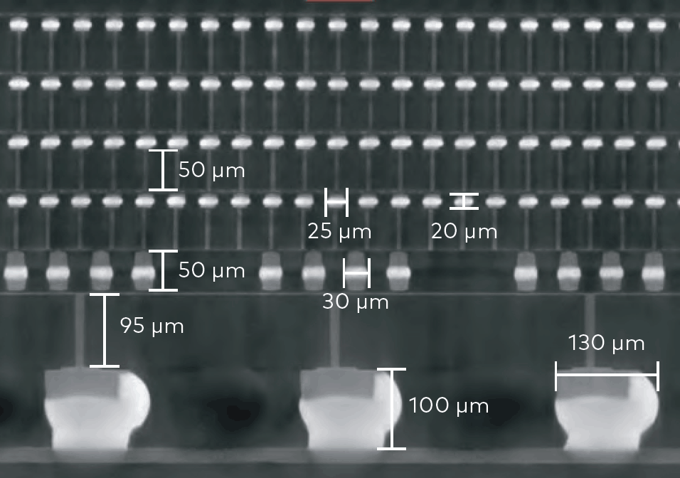
For example, inside a 12mm x 8mm semiconductor HBM package, Φ25µm microbumps and Φ5µm TSVs (Through-Silicon Vias) are densely packed. Conventional X-ray CT systems was extremely difficult to clearly separate and observe voids, cracks, or connectivity failures in these microstructures.
The true value of Comet’s FF35 CT lies in the details. The detail visibility of 0.6µm (600nm) is consistently delivered by utilizing the newly available 160kV nanofocus tube “FYNE Tube” which clearly visualize and measure fine wiring and defects inside bumps that were previously invisible.
Details of the New 160kV Nanofocus Tube “FYNE Tube”
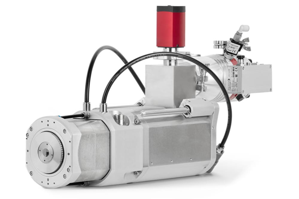
The “FYNE Tube (FYT-160.NFX1.600)”, which can now be installed as the heart of the FF35 CT, is a next-generation 160kV open-type nanofocus tube featuring a state-of-the-art LaB6 (lanthanum hexaboride) emitter. In the inspection of semiconductors and ultra-precise electronic components, two conflicting factors have always been demanded: “extremely high resolution” to capture minute defects and “stable, long-duration continuous operation” to maintain throughput on the production floor.
With conventional X-ray tubes, users had to choose between “open tubes” which offer high resolution but require frequent maintenance such as filament changes, and “sealed tubes” which are maintenance-free but have limited resolution. However, the FYNE Tube breaks down the barrier between the two with a revolutionary design, successfully fusing “the overwhelming high resolution of an open tube” with “stability and low maintenance comparable to a sealed tube”. This minimizes downtime in the inspection process while continuously providing insights of the highest level, dramatically improving yield and quality assurance reliability. It features the following outstanding characteristics:
-
1. Sharp Focal Spot and High Output with 0.6 µm Spatial Resolution
It boasts top-class output while maintaining nano-resolution. Because high-output, bright images can be obtained while keeping the focal spot size under 1µm, edges do not blur even at sub-micron voxel levels, ensuring reliable visualization of fine details down to 600nm (0.6µm).
-
2. Minimal Thermal Drift Ideal for Long Scans
Thermal drift, a common challenge in high-magnification CT scanning, is suppressed to an extremely low level by the water-cooled tube head. Featuring ultimate repeatability, it is ideal for inspecting samples that require long scans or continuous operation.
-
3. Long Service Life and Low Maintenance
It achieves a long service life, dramatically reducing maintenance frequency compared to conventional open-tube systems. This maintains high utilization rates and significantly contributes to lowering total cost of ownership (TCO).
Breakthrough “Zoom Scan” Technology
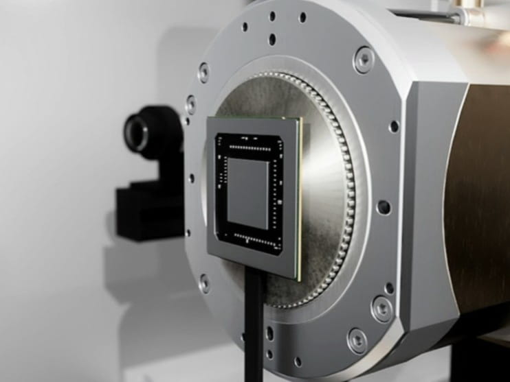
To achieve high magnification (high resolution), it is necessary to bring the sample as close as possible to the X-ray tube (Focus) (minimizing the FOD). However, rotating wide samples like PCBs would cause collisions with the X-ray tube. Therefore, in the past, users had to position the sample further away to allow rotation (normal scan), resulting in a loss of resolution.
The “Zoom Scan” of the FF35 CT solves this dilemma. It is a revolutionary function that dynamically adjusts the distance between the sample and the X-ray source for each angle, getting as close as possible whenever allowed. This enables efficient high-magnification imaging even for large PCBs.
How Zoom Scan Works
To achieve high-resolution CT, the sample must be brought as close as possible to the “X-ray Tube” on the left.
Zoom Scan dynamically adjusts the distance according to the rotation, constantly keeping the closest approach for maximum magnification.
Conventional Normal Scan
The sample rotates while maintaining a safe, distant clearance to prevent its corners from colliding with the X-ray tube. As a result, the magnification ratio remains low.
Zoom Scan
The sample automatically approaches the X-ray tube when its shorter side faces it, and backs away to avoid collision when the longer side faces it. The average magnification increases dramatically.
Streamlining Analysis with the Software Suite
The FF35 CT features industry-leading software as well as top-tier hardware. Utilizing the AI-based 3D software “Dragonfly 3D World” enables automatic segmentation powered by deep learning. It quickly analyzes the volume and surface area of millions of pores and voids in semiconductor packages, drastically reducing manual data processing effort.
Installation in Thailand
As new factory investments and industrial upgrading progress in Thailand, the installation of not only production equipment but also advanced inspection systems is a critical key to future competitiveness. The new nanofocus tube “FYNE Tube” and the intelligent scanning technologies equipped on the FF35 CT will reliably resolve our customers’ challenges of “wanting to see the unseen” in semiconductor and electronics manufacturing.
As Comet’s sales agent in Thailand, we are pleased to support your inquiries for installing the FF35 CT. For after-sales support and technical maintenance, you can rest assured as Comet’s manufacturer-direct technical team is permanently stationed in Thailand.
We also welcome inquiries for sample evaluation and scan demonstrations using your actual specimens. If you have any questions, such as “Can this fine crack be seen?” or “Can high resolution be maintained with our specific board size?”, please feel free to contact us.
Would you like a demo or detailed materials for the FF35 CT?
Our dedicated sales staff in Thailand will propose the optimal installation plan tailored to your specific inspection requirements.
 Non-Destructive Testing (Industrial X-ray CT) Systems